- 您现在的位置:买卖IC网 > Sheet目录1219 > HI3026EVAL (Intersil)EVALUATION PLATFORM HI3026
�� �
�
�Application� Note� 9652�
�Board� Adjustments� and� Settings�
�1.�
�2.�
�3.�
�4.�
�5.�
�6.�
�VRB.R1:�
�VRT.R2:�
�OFFSET.R3:�
�FULL� SCALE.R4:�
�FULL� SCALE.R5:�
�S1:�
�HI3026,� VRB� voltage� adjusting� volume.�
�HI3026,� VRT� voltage� adjusting� volume.�
�Adjusting� volume� for� matching� the� AMP.IN� input� and� DIR.IN� input� signal� ranges� to� the�
�HI3026,� input� range.�
�Full-scale� adjusting� volume� for� the� port� 1� D/A� output.� (-1V:� Typ.)�
�Full-scale� adjusting� volume� for� the� port� 2� D/A� output.� (-1V:� Typ.)�
�Switching� junction� for� the� dual� analog� input� pins.�
�Set� as� follows� according� to� the� input� pins� used.�
�JUNCTION�
�SYMBOL�
�AMP.IN�
�DIR.IN�
�A�
�OPEN�
�0.1� μ� F�
�B�
�SHORT�
�10k� ?�
�7.�
�8.�
�9.�
�10.�
�S2:�
�SW1� SELECT:�
�SW2� A/D� INV:�
�SW#� D/A� INV:�
�Setting� junction� for� the� clock� frequency� division� ratio.� The� operating� speed� after� latching� is�
�determined� by� the� frequency� division� ratio� set� here.�
�When� set� to� CLK� OUT,� it� operates� according� to� the� HI3026,� clock� output.�
�HI3026,� output� mode� selector� switch.�
�HI3026,� output� polarity� inversion� switch.�
�D/A� converter� output� polarity� inversion� switch.�
�Notes� on� Board� Operation�
�1.�
�The� factory� settings� for� the� HI3026,� Evaluation� Board�
�are� as� follows:�
�3.�
�When� the� analog� input� signal� is� a� sine� wave� or� other�
�repeating� waveform,� the� signal� can� be� input� form� the�
�CON2� (DIR.IN)� pin� with� AC� coupling.� In� these� cases,�
�VRB.R1� =� 1.5V�
�VRT.R2� =� 3.0V�
�OFFSET.R3� =� 2.25V�
�FULL� SCALE.R4� =� -1V� S1� A···OPEN,�
�B� ···SHORT�
�FULL� SCALE.R5� =� -1V� S2� 8···SHORT�
�(1/8� frequency�
�division)�
�4.�
�the� input� dynamic� range� is� not� limited� by� the� +AMP� and�
�-AMP� supply� voltages,� but� the� VRT� level� may� be� limited�
�by� IC3:NJM3403A.� Therefore,� the� power� supply� for� the�
�operational� amplifier� should� be� shifted� in� the� same�
�manner� as� in� 2.� above.�
�In� the� evaluation� board� of� the� HI3026,� CLC404� (Comlin-�
�2.�
�When� using� the� board� in� this� condition,� the� input� signals�
�should� be� input� at� the� amplitudes� shown� below.�
�(The� frequency� is� set� as� desired.)�
�When� the� analog� signal� is� input� from� the� CON1�
�(AMP.IN)� pin,� IC2:CLC404� limits� the� input� dynamic�
�range� of� the� A/D� converter’s� analog� input� signal� accord-�
�ing� to� the� +AMP� and� -AMP� supply� voltages.� The� power�
�supply� for� the� operational� amplifier� can� also� be� shifted�
�to� +AMP� =� +7.0V� and� -AMP� =� -3.0V� to� allow� use� with� a�
�wider� input� dynamic� range.�
�ANALOG� INPUT� SIGNAL:� CON1� (AMP.IN)�
�CLOCK� INPUT� SIGNAL:� CON3� (CLK.IN)�
�5�
�ear)� is� employed� for� IC2� to� drive� the� analog� input� signal.�
�Though,� CLC505� (Comlinear)� can� also� be� used� instead�
�of� CLC404,� there� should� be� little� change� in� the� periph-�
�eral� circuit� in� this� case.�
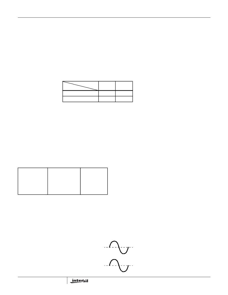
�0V� CENTER,� 800mV� P-P� OR� LESS�
�0V� CENTER,� 1.0V� P-P�
�发布紧急采购,3分钟左右您将得到回复。
相关PDF资料
HI5746EVAL1
EVALUATION PLATFORM HI5746
HIP1011AEVAL1
EVAL BOARD PCI HOT PLUG HIP1011
HIP1011DEVAL1
EVAL BOARD PCI HOT PLUG DUAL
HIP1011EVAL1
PCI HOT PLUG EVALUATION BOARD
HIP1011EVAL2
EVAL BOARD COMPACT PCI HOT PLUG
HIP1012EVAL1
EVALUATION BOARD DUAL GENERIC
HIP1013EVAL1
EVALUATION BOARD DUAL GENERIC
HIP2100EVAL2
EVAL BOARD 48VDC-5UDC CONVERTER
相关代理商/技术参数
HI3026JCQ
功能描述:ADC FLASH 8BIT 120MSPS 48-PQFP RoHS:是 类别:集成电路 (IC) >> 数据采集 - 模数转换器 系列:- 产品培训模块:Lead (SnPb) Finish for COTS
Obsolescence Mitigation Program 标准包装:2,500 系列:- 位数:12 采样率(每秒):3M 数据接口:- 转换器数目:- 功率耗散(最大):- 电压电源:- 工作温度:- 安装类型:表面贴装 封装/外壳:SOT-23-6 供应商设备封装:SOT-23-6 包装:带卷 (TR) 输入数目和类型:-
HI-303
制造商:INTERSIL 制造商全称:Intersil Corporation 功能描述:Dual, SPDT CMOS Analog Switch
HI-303/883
制造商:INTERSIL 制造商全称:Intersil Corporation 功能描述:Dual SPDT CMOS Analog Switch
HI303005
制造商:Harris Corporation 功能描述:
HI3-0300-5
制造商:Harris Corporation 功能描述:
HI30300-5
制造商:Rochester Electronics LLC 功能描述:- Bulk
HI3-0301-5
制造商:Rochester Electronics LLC 功能描述:- Bulk
HI3-0302-5
制造商:Rochester Electronics LLC 功能描述:- Bulk